
What is HBM Memory? The Stacked Chip Behind AI Hardware
Quick Summary:
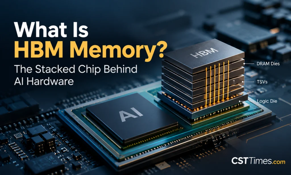
HBM memory, short for High Bandwidth Memory, is computer memory built by stacking several DRAM chips on top of each other and placing the stack right beside a processor. This short, wide connection lets data move between memory and chip much faster than ordinary memory modules can manage. That is why HBM sits inside most advanced AI accelerators. This guide explains how HBM works, how it compares with DDR5 and GDDR, how it has evolved from HBM1 to HBM4, and why it affects both the AI boom and everyday memory prices.
Table of Contents
ToggleKey Takeaways
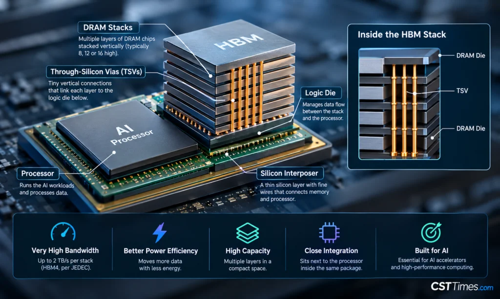
- HBM stacks DRAM chips vertically and links them with tiny vertical connections called through-silicon vias (TSVs).
- Its advantage is a very wide data path. The HBM4 standard uses a 2,048-bit interface per stack.
- According to JEDEC, HBM4 reaches up to 2 TB/s per stack, and some vendors rate their parts higher.
- Only three companies make HBM at scale: SK hynix, Samsung, and Micron.
- HBM uses much more wafer capacity per gigabyte than standard DRAM, which analysts link to tighter supply and higher prices for ordinary memory.
How HBM Memory Works
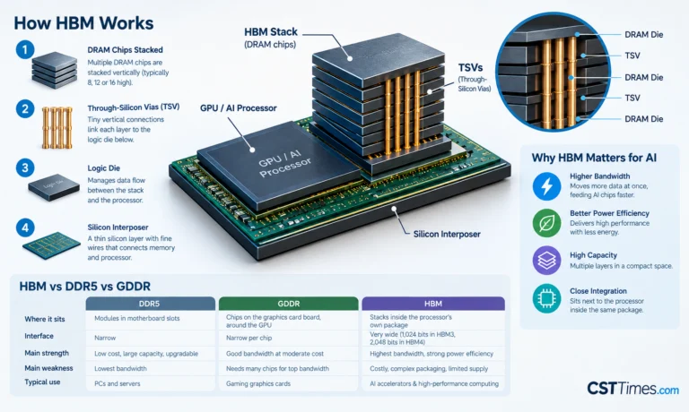
A processor can only work as fast as data reaches it. In a traditional setup, memory chips sit on modules or around the processor on a circuit board, and the wires between them are long and narrow. HBM redesigns that layout in three steps.
First, the DRAM chips are stacked, typically 8, 12, or 16 layers high. Second, microscopic vertical channels called through-silicon vias connect each layer to the next and to a logic chip at the base of the stack. Third, the finished stack sits next to the processor on a silicon interposer, a thin piece of silicon packed with fine wires, so memory and processor live in one package.
Think of bandwidth, the amount of data moved per second, as traffic on a road. Ordinary memory is a few very fast lanes. HBM is thousands of lanes running at more moderate speeds, so far more traffic gets through. Bandwidth is measured in gigabytes per second (GB/s) or terabytes per second (TB/s), and one terabyte equals 1,000 gigabytes.
HBM vs DDR5 vs GDDR
All three are DRAM-based, but they are built and placed differently.
| DDR5 | GDDR | HBM | |
|---|---|---|---|
| Where it sits | Modules in motherboard slots | Chips on the graphics card board, around the GPU | Stacks inside the processor’s own package |
| Interface | Narrow | Narrow per chip | Very wide per stack (1,024 bits in HBM3, 2,048 in HBM4) |
| Main strength | Low cost, large capacity, upgradable | Good bandwidth at moderate cost | Highest bandwidth per package, strong power efficiency |
| Main weakness | Lowest bandwidth of the three | Needs many chips to reach top bandwidth | Costly, complex packaging, limited supply |
| Typical use | PCs and servers | Gaming graphics cards | AI accelerators and high-performance computing |
The trade-off is cost and flexibility. DDR5 modules can be swapped or upgraded, while HBM is permanently attached to its processor package. GDDR remains the common choice for gaming graphics cards because it is cheaper and simpler to build.
HBM Generations: HBM1 to HBM4
HBM is older than most people think. JEDEC adopted the first HBM standard in October 2013, and AMD’s Fiji graphics chips were the first devices to use it in 2015. Each generation since has raised bandwidth per stack.
| Generation | Peak bandwidth per stack | Key detail |
|---|---|---|
| HBM1 | 128 GB/s | 4 GB stacks, 1 Gb/s per pin |
| HBM3 | About 819 GB/s | 6.4 Gb/s per pin, 1,024-bit interface |
| HBM3E | Up to about 1.2 TB/s | Micron quoted 24 GB in an 8-high stack |
| HBM4 | Up to 2 TB/s (JEDEC baseline) | 2,048-bit interface; some vendor parts rated above 2.8 TB/s |
Selected generations only. These are peak ratings, not real-world averages.
The big change in HBM4, published by JEDEC in April 2025, is that the interface doubled from 1,024 to 2,048 bits, with speeds up to 8 Gb/s per pin. Memory makers have pushed beyond that baseline. Micron says its 36 GB, 12-high HBM4 stack is in volume shipment, running above 11 Gb/s per pin for more than 2.8 TB/s. A successor, HBM4E, is expected to follow.
Why AI Chips Need HBM
Large AI models must read enormous amounts of data from memory again and again. If memory is too slow, the processor’s compute cores sit idle waiting for data. HBM keeps those cores fed, which is why AI accelerators are designed around it.
Nvidia’s Rubin platform shows the scale. Each Rubin GPU package carries eight HBM4 stacks with 288 GB of capacity and up to 22 TB/s of bandwidth. Dividing by eight gives roughly 2.75 TB/s per stack, our own calculation. Spec summaries put that at about 2.75 times the 8 TB/s of Nvidia’s previous Blackwell generation.
Short distances also save energy, which matters when data centers run thousands of chips. Micron says its HBM4 is more than 20% more power-efficient than HBM3E.
Who Makes HBM in 2026
Only three companies can make HBM at scale: SK hynix, Samsung Electronics, and Micron. SK hynix leads. In its SEC filing, citing IDC, it reports a 56.4% share of HBM revenue in the first quarter of 2026. Revenue share and bit share differ, so other trackers show other numbers. TrendForce projected SK hynix at about 50% of 2026 HBM bit output.
On June 5, 2026, Nvidia CEO Jensen Huang said all three suppliers had passed certification to provide HBM4 for Rubin, according to Investing.com. Samsung began HBM4 mass production in February 2026. A September report says SK hynix has started mass-producing a 16-layer, 48 GB HBM4 part, while Micron has shipped samples of that taller design. This market moves fast, so treat any ranking as a snapshot.
Why HBM Is Costly and Affects Memory Prices
HBM is hard to manufacture. Makers must thin DRAM chips, drill TSVs, and bond many layers precisely, and one defect can spoil a whole stack. That building 16-layer stacks reliably is a key challenge, and the three makers use different bonding methods.
HBM also uses more silicon. EE Times reports that HBM3E takes about three times as much wafer space as standard DDR5. Factories have limited capacity, so wafers used for HBM cannot make everyday memory. Analysts link this shift, alongside broader AI demand, to sharply higher DRAM prices in 2026. One analysis expects the squeeze to ease by 2027–2028, though forecasts vary.
The practical result is that laptops, phones, and PC memory kits can cost more even though they contain no HBM. In short, HBM offers top-tier bandwidth, strong power efficiency, and a compact footprint. Its limits are high cost, complex packaging, tight supply, and no upgradability.
Final Thoughts:
HBM is not simply a faster version of the RAM in a laptop. It is a different way of building memory and placing it beside the processor. That design solves the data-delivery problem that limits AI hardware, but it comes with higher cost and tighter supply. Those trade-offs now shape both AI chip availability and memory prices.
FAQs
Is HBM the same as RAM?
HBM is a form of DRAM, the same basic memory type used in ordinary RAM. What differs is the packaging: stacked chips, a very wide interface, and placement beside the processor.
Can I install HBM in my PC?
No. HBM is built into the processor’s package, so it cannot be added or upgraded like a memory module.
Is HBM4 the newest version?
HBM4 is the newest generation in production as of October 2026. HBM4E is expected to come next.
Will HBM make my phone or laptop faster?
Not directly. Consumer devices mostly use LPDDR or DDR memory. HBM mainly serves data-center AI and high-performance computing, though it affects consumer memory prices through shared factory capacity.
